Physically describe the behavior of the charge carriers and ionized dopant atoms in the vicinity of a semiconductor pn junction that causes the potential (energy) barrier that tends to prevent charge carriers from crossing the junction.
What will be an ideal response?
Analysis:
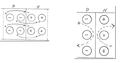
Semiconductor atoms are not shown in the two figures. The circles represent ionized dopant atoms and the uncircled plus and minus signs represent charge carriers. The dotted line in the first figure represents how far the depletion/space charge region extends into the P and N regions.
Near the junction, the negative carriers in the N material recombine with the positive carriers in the P material. This forms a small region on either side of the junction which is depleted of charge carriers; however, the ionized dopant atoms are immobile and remain. Therefore, in the N material the region has a net positive charge and in the P material the region has a net negative charge. This region is called either a "depletion" region [depleted of carriers] or a "space charge" region [due to the dopant ions].
If a conduction band free electron [a majority carrier] in the N material tries to cross into the P material, it encounters and is repelled by the net negative charge [due to the ionized acceptor atoms] in the depleted part of the P material.
If a valence band hole [a majority carrier] in the P material tries to cross into the the N material, it encounters and is repelled by the net positive charge [due to the ionized donor atoms] in the depleted part of the N material.
The repulsion of the carriers is characterized as a Coulombic "potential [energy] barrier". With no voltage applied across the junction, Ohm's law requires the current to be zero. Actually, very, very small equal but opposite currents do flow across the junction but the net curent is zero.
The barrier can be decreased by applying a "forward bias" voltage across the junction. This allows more carriers to cross the junction and when this voltage is greater than a certain value [0.7 V for Silicon] a significant current [milliamps] flows.
The barrier can be increased by applying a "reverse bias" voltage across the junction. This increases the barrier and fewer majority carriers have sufficient energy to cross the junction, i.e., the current essentially ceases. However, there is a VERY, VERY small "reverse saturation current" [in the femtoamps range] due to the minority carriers. Since the minority carriers are thermally produced, this current is dependent on temperature.
You might also like to view...
All of the following can help the supervisor use the estimated cost to control costs and resources on the job except _____.
a. supplying information for standard project costs b. providing labor and equipment production rates c. determining how the budget will track costs d. evaluating the efficiency of construction operations
The center of the cone, pod, nut, and fruit wreath is left open and filled with _____ placed upside down
A) nuts B) seeds C) pine cones D) all of the above
The standard transformer VA rating for most HVACR systems is:
A) 60 VA. B) 20 VA. C) 100 VA. D) 40 VA.
Phantom loads, also referred to as ____, are the small amounts of electricity that many appliances and electronics use even when they appear to be turned off.
A. ghosts B. spirits C. vampires D. angels