Consider the circuit below. Assume that all gates are implemented in silicon by NAND gates, NOR gates and inverters. Each NAND gate, NOR gate, or inverter has an internal delay of 0.4 ns. A logic transition at an input may cause a change at the output (depending on other inputs and the circuit). The time for a transition at the input to appear as a corresponding transition at an output depends on the circuit path and the nature of the gates. What is the longest circuit path through this circuit and what is the worst case delay that a signal experiences going through the circuit?
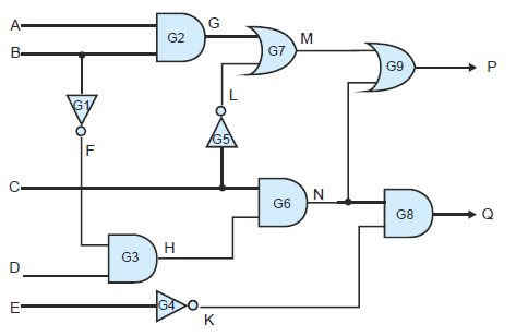
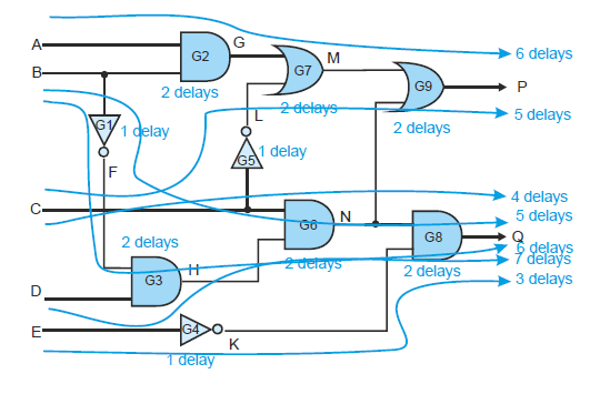
The following diagram demonstrates all the paths through this circuit and their delays. Remember an AND gate is a NAND gate plus an inverter (and an OR gate is a NOR gate plus an inverter). Consequently, all AND and OR gates suffer two delay units. The longest path is from B via G1, G3, G6, G8 and is 7 delays or 7 × 0.4 = 2.8 ns.
You might also like to view...
Write a void function using two type int call-by-reference parameters that swaps the values in the arguments. Be sure to include testable pre and post conditions.
What will be an ideal response?
Show the tree that is the result of removing the following elements (in order): 13, 16, 12.
Consider the following binary search tree. 12 / \ 9 16 / / \ 1 13 15
Which security mode allows two or more classification levels of information to be processed at the same time?
A. Dedicated B. System High C. Compartmented D. Multilevel
The simplest C selection statement is the one-way if statement.
Answer the following statement true (T) or false (F)