Given the timing diagram below which is derived from the data sheet of a commercial SRAM, explain its action in words.
Timing diagram of a SRAM memory
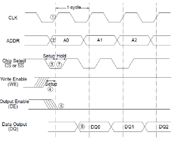
This is a read cycle because the write enable signal, WE*, is inactive?high (i.e., negated) for three cycles. The key event is the assertion of the active?low chip select, CS*, on the rising edge of the first clock. When CS* goes active low, an access is triggered. Note that CS* must go low before the rising edge of the clock (setup
time) and remain low until the hold time after the rising edge.
The write enable must be high before the rising edge of the clock for its setup time to recognize a read cycle. Similarly, the output enable, OE*, must become active?low before the rising edge of the clock. If WE* remains high and OE* low, then data is put on the data bus in each clock cycle. In each case the address must be valid
before each rising edge of the clock.
You might also like to view...
Does it make sense to initialize condition variables?
What will be an ideal response?
The Select Image Source dialog box opens when the Images button arrow on the Common tab of the Insert panel is clicked and then the ____________________ button is clicked.
Fill in the blank(s) with the appropriate word(s).
________ are saved text and objects that can be retrieved and inserted into documents quickly
Fill in the blank(s) with correct word
Class data members are ____________________ in scope to objects created from the class.
Fill in the blank(s) with the appropriate word(s).